Buck Converter
The purpose of this exercise was to review basic buck converter design. I originally learned this in class at Purdue but have not used it in 4 years and needed a refresher. I will continue this exercise with further reviews on other power converter topologies.
I chose components and a scenario that is maybe not the most elementary buck converter design, but this forced me to consider aspects of design I would have otherwise missed.
With some help from a Texas Instruments PDF and the web, I calculated the Inductor and Output Cap from a parameter list I defined. I approached these parameters with an eMotor/electromagnetic background and intentionally chose a low resistance load.

Hand Calculations for Cout and L
Next Step was to create a model in LTspice. I started with generic spice components and improvised from there.

LTspice Model
The generic components I started with were not working correctly, I believe this was due to the large current draw and low pulse voltage. This led me to find appropriate components for the output current I calculated (33A). I chose a Schottky diode with an average forward current of 40 Amps and 30V breakdown voltage. I then changed to an N-type mosfet with a 42A continuous current rating. These component changes with an extended simulation window to overcome the transient time for the large passive components finally gave me some results close to what I was looking for.

Outputs Measured At the Load

Steady State Values
As you can see above, the transient is pretty long, around 60-70ms. This was expected with a 10mF cap and 2.2mH inductor on the output. There could be controls or design changes implemented depending on the use cases to help mitigate this transient time.
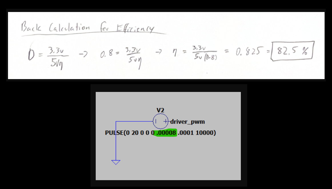
Duty Cycle and Efficiency
From my estimations, the efficiency at this operating point is around 82.5%. I started out by calculating a duty cycle with an assumption of 90% efficiency, the output was around 3.0V. I manually adjusted the “Ton” parameter of the gate driver to achieve the desired output of 3.3V. The duty cycle that achieved 3.3V was 80%. I then plugged this back into the duty cycle equation and solved for the efficiency parameter. In ideal calculations it would be 66%, which highlights the inefficiencies of this design. My assumptions are that these losses mainly come from the switch and diode.
I plan to revisit this design and try implementing improvements to increase efficiency. This would include plotting the losses on the diode vs the MOSFET at different duty cycles and evaluating the effect of replacing the diode with a switch. It might come down to needing a more efficient MOSFET with a lower Rds(on).
Websites and documents used: